Monday, September 30, 2013
Simple But Reliable Car Battery Tester
This solution is better than letting the internal voltage regulator set the 12V sample voltage to be feed into the internal voltage divider simply because it cannot regulate 12V when the voltage drops lower (linear regulators only step down). Simply wiring with no adjust, the regulator provides stable 1,25V which is fed into the precision internal resistor cascade to generate sample voltages for the internal comparators. Anyway the default setting let you to measure voltages between 8 and 12V but you can measure even from 0V to 12V setting the offset trimmer to 0 (but i think that under 9 volt your car would not start).

There is a smoothing capacitor (4700uF 16V) it is used to adsorb EMF noise produced from the ignition coil if you are measuring the battery during the engine working. Diesel engines would not need it, but Im not sure. If you like more a point graph rather than a bar graph simply disconnect pin 9 on the IC (MODE) from power. The calculations are simple (default)
For the first comparator the voltage is : 0,833 V corresponding to 8 V
* * * * * voltage is : 0,875 V corresponding to 8,4 V
for the last comparator the voltage is : 1,25 V corresponding to 12 V
Have fun, learn and dont let you car battery discharge... ;-)
e-mail: jonathan.filippi@virgilio.it
Fine Control Super Bright LED Pulser
This circuit, designed on request for a Halloween prop, allows fine control of a pulsing Super Bright white LED. The four potentiometers or trimmers will set precisely: on, off, ramp up and ramp down time-delays respectively. Ramp up and ramp down time-delays can be set roughly in the 1 - 15 seconds range, whereas on and off time-delays can range from a few seconds to about one minute. A 12V battery or regulated power supply is required, provided it is reasonably stable. Total current drawing is about 25 - 30mA when the LED reaches maximum brightness.
 Parts:
R1,R5,R12,R13___10K 1/4W Resistors
R2,R5___________10K 1/2W Trimmers or Lin. Potentiometers
R3______________47K 1/4W Resistor
R4______________22K 1/4W Resistor
R6_______________1K 1/4W Resistor
R7,R8,R9,R14___100K 1/4W Resistors
R10,R11__________2M2 1/2W Trimmers or Lin. Potentiometers
R15____________220R 1/4W Resistor
C1,C2__________100nF 63V Polyester or ceramic Capacitors
C3,C4___________22µF 25V Electrolytic Capacitors
C5_____________220µF 25V Electrolytic Capacitor
D1,D2________1N4148 75V 150mA Diodes
D3______________LED Super Bright white (e.g. RL5-UV2030)
Q1____________BC337 45V 800mA NPN Transistor
IC1___________LM324 Low Power Quad Op-amp IC
IC2____________4093 Quad 2 input Schmitt NAND Gate IC
Notes:
- Wanting to use two white LEDs, the second device must be wired across the Emitter of the transistor and negative ground with its own limiting resistor wired in series, like R15 and D3 in the circuit diagram.
- If common red, yellow or green LEDs are required, please wire two of them in series, in order to present roughly the same voltage drop of one white or blue LED.
- Please note that the unused sections in both ICs must have their inputs tied to negative ground whereas the outputs must be left open, as shown at the bottom of the diagram.
- All time-delays can be increased by changing the value of C3 and C4 to 47µF 25V or even higher. Please vary the value of these capacitors only, as the values of the resistors wired to the four control pots are rather critical and should not be changed.
Sunday, September 29, 2013


Saturday, September 28, 2013
One second Audible Clock Circuit

R1 = 10K
R2 = 47.K
R3 = 100R
C1 = 1nF-63V
C2 = 10µF-25V
C3 = 100nF-63V
D1 = 1N4148
D2 = 1N4148
D3 = 1N4148
D4 = LED-(Optional, any shape and color, see Notes)
D5 = 1N4148-75V 150mA Diode (Optional, see Notes)
Q1 = BC337-45V 800mA NPN Transistor
IC1 = 4024-7 stage ripple counter IC
BZ1 = Piezo sounder (incorporating 3KHz oscillator)
SPKR = 8 Ohm, 40 - 50mm diameter Loudspeaker (Optional, see Notes)
SW1 = SPST Toggle or Slide Switch (Optional, see Notes)
B1 = 3 to 12V Battery (See Notes)
Notes:
- To allow precise circuit operation in places where the mains supply frequency is rated at 60Hz, the circuit must be modified as follows: disconnect the Cathode of D1 from pin #11 of IC1 and connect it to pin #9. Add a further 1N4148 diode, connecting its Anode to R1 and the Cathode to pin #6 of IC1: thats all!
- The circuit will work fine with battery voltages in the 3 -12V range.
- The visual display, formed by D4 and R3 is optional. Please note that R3 value shown in the Parts list is suited to low battery voltages. If 9V or higher voltages are used, change its value to 1K.
- If a metronome-like click is needed, R2 and BZ1 must be omitted and substituted by the circuit shown enclosed in dashed lines, right-side of the diagram.
- Stand-by current drawing is negligible, so SW1 can be omitted.
1995 Buick Park Avenue Wiring Diagram
 |
| 1995 Buick Park Avenue Wiring Diagram |
Friday, September 27, 2013
Direction Sensitive Light Barrier

Both types of installation are shown here, which one is most suitable depends on the actual application. When used in a doorway, one transmitter is sufficient if the receivers are placed about 5 cm apart. With a wider passage, an installation with two separate IR-transmitters is a better solution. This circuit has a range of several meters, even if the sun shines directly on the receiver! We use the exact same IR-transmitter(s) as for the modulated light barrier. For the installation with two separate IR-transmitters it is sufficient to duplicate R6, T1, D1, C3 and R7 from the circuit of the modulated light barrier.

Output OUT (pin 3) of IC2 can drive two of these IR-drivers without any difficulty. The receivers are slightly different than those of the modulated light barrier and the circuit is the same for both types of installation. We again use the TSOP1736, which is sensitive to IR-light that is modulated at a frequency of 36 kHz. D2, R8 and C4 ensure that the received pulses from IC3 at the output of IC5a result in a ‘1’ when the beam is not interrupted. When the beam is interrupted this output will become a ‘0’ within about 1 ms.
In the same way IC5b generates a ‘0’ when IC4 stops receiving IR-light. The 4013 CMOS-IC used here contains two D-flipflops, of which we use only one. The instant that light barrier 2 (IC4) is unblocked again, is used to clock the state of light barrier 1 (IC3) through to output Q1. This signal drives the relay via T2, which operates the light in the room. The circuit therefore turns the light on or off the moment that light barrier 1 is uninterrupted.
Switch Timer Circuit For Bathroom Light

Thursday, September 26, 2013
ESR Low Resistance Test Meter
As electrolytic capacitors age, their internal resistance, also known as "equivalent series resistance" (ESR), gradually increases. This can eventually lead to equipment failure. Using this design, you can measure the ESR of suspect capacitors as well as other small resistances. Basically, the circuit generates a low-voltage 100kHz test signal, which is applied to the capacitor via a pair of probes. An op amp then amplifies the voltage dropped across the capacitor’s series resistance and this can be displayed on a standard multimeter. In more detail, inverter IC1d is configured as a 200kHz oscillator.
Its output drives a 4027 J-K flipflop, which divides the oscillator signal in half to ensure an equal mark/space ratio. Two elements of a 4066 quad bilateral switch (IC3c & IC3d) are alternately switched on by the complementary outputs of the J-K flipflop. One switch input (pin 11) is connected to +5V, whereas the other (pin 8) is connected to -5V. The outputs (pins 9 & 10) of these two switches are connected together, with the result being a ±5V 100kHz square wave. Series resistance is included to current-limit the signal before it is applied to the capacitor under test via a pair of test probes. Diodes D1 and D2 limit the signal swing and protect the 4066 outputs in case the capacitor is charged.
Circuit diagram:
 ESR & Low Resistance Test Meter Circuit Diagram
A second pair of leads sense the signal developed across the probe tips. Once again, the signal is limited by diodes (D3 & D4) before begin applied to the remaining two inputs of the 4066 switch (pins 2 & 3 of IC3a & IC3b). These switches direct alternate half cycles to two 1μF capacitors, removing most of the AC component of the signal and providing a simple "sample and hold" mechanism. The 1μF capacitors charge to a DC level that is proportional to the test capacitor’s ESR. This is differentially amplified by op amp IC4 so that it can be displayed on a digital multimeter – 10Ω will be represented by 100mV, 1Ω by 10mV, etc. To calibrate the circuit, first adjust VR1 to obtain 100kHz at TP3.
Next, momentarily short the test probes together and adjust VR4 for 0mV at pin 6 of IC4. That done, set your meter to read milliamps and connect it between TP4 and the negative (-) DMM output. Apply -5V to TP2 and note the current flow, which should be around 2.1mA. Transfer the -5V from TP2 to TP1 and adjust VR2 until the same current (ignore sign) is obtained. Remove the -5V from TP1. Again, set to your meter to read volts and connect it to the DMM outputs. Apply the probes to a 10W resistor and adjust VR3 for a reading of 100mV. Finally, ensure that all capacitors to be tested are always fully discharged before connecting the probes.
Author: Len Cox - Copyright: Silicon Chip Electronics
ALTERNATING FLASHER ELECTRONIC DIAGRAM

The first IC used as a 1 second clock, which generates ON/OFF for the other ICs. Diodes help to cover the IC555 from the peak voltage. Take note that the relay used should have impedance more than 50 ohm.
Parts list :
- Diode D1-D2 : 1N4001
- Zener Diode D2 : 6V
- R1,R5,R7 : 3k3
- R2,R6,R8 : 68k
- Resistor variable VR1 : 47k
- Polar capacitor C1 : 10uF/16V
- Polar capacitor C3,C5 : 2.2 uF/16V
- Capacitor C2,C4,C6 : 0.01 uF
- Transistor T1 : BC107/BC148
- IC timer : NE555
- Relay : 6-9 V
- Power supply 6-9 V
Wednesday, September 25, 2013
Low Cost Battery Condition Indicator

The series resistor for the LED needs to be selected for each battery voltage, to limit the current to a safe vale or you could use a fixed resistor and a series trimpot for flexibility. Low battery voltage is indicated by the LED pulsing at around 1Hz. The battery voltage is monitored by transistor Q1 and trimpot VR1. Once the voltage at its base falls below 0.6V, Q1 turns off and Q2 turns on to enable the 2-gate oscillator formed by IC1a and IC1b, which runs at 1Hz. The pulses from this oscillator are inverted by IC1d to gate the LED oscillator on and off. Calibration can be done with a variable bench power supply set to the lowest battery voltage you will accept. Power up the circuit and adjust VR1 until the LED pulses once per second.
1983 Ford Bronco Wiring Diagram
 |
| 1983 Ford Bronco Wiring Diagram |
switch, resistance wire, horn relay, alternator, relay, stop light switch, fuse box, directional flasher, low brake, hazard flasher, coolant temp switch, high beam, fuel gauge, license lights, red wire, tail light, instrument light
Tuesday, September 24, 2013
Automatic Headlight Reminder
The circuit works like this:
when the ignition is on, transistor Q1 is also on and this pulls pin 4 of IC1 low. As a result, IC1 is held reset and no clock pulses are fed to IC2. Conversely, if the ignition is turned off, Q1 will turn off and so IC1 will start oscillating and sound the piezo siren. At the same time, IC1 will clock IC2 and so LEDs 1-10 will light in sequence and stop (after about 10s) with the last LED (LED10) remaining on. Thats because, when IC2s O9 output (ie, pin 11) goes high, Q2 also turns on and this pulls pin 4 of IC1 low, thus stopping the oscillator (and the siren).

Note:
That different colored LEDs are used to make the display look eye-catching but you make all LEDs the same color if you wish. Installing optional diode D1 will alter IC1s frequency and this will alter the display rate. Finally, if the lights are turned off and then back on again, the alarm will automatically retrigger. LED1 is always on if the lights are turned on. If you dont want the LED display, just leave the LEDs out.
Automatic Light Dimmer

The light then comes on. When the light switch is turned off, C2 is discharged via P1, R2 and D6. When the potential across C2 drops, the brightness of the LED diminishes, so that the p.d. across R3 also drops. The increasing resistance of R3 effects phase angle control of the triac so that the light is dimmed gradually. The dimming time may be altered with P1 within the time range determined by network R2-C2. The circuit operates correctly only, of course, when the LDR is not exposed to light other than that from the LED. The type of LDR is not particularly important, as long as it is not too long: in the prototype, a model with a length of 5 mm was used.
Monday, September 23, 2013
22 Watt Car Subwoofer Amplifier
22W into 4 Ohm power amplifier, Variable Low Pass Frequency: 70 – 150Hz
This unit is intended to be connected to an existing car stereo amplifier, adding the often required extra "punch" to the music by driving a subwoofer. As very low frequencies are omnidirectional, a single amplifier is necessary to drive this dedicated loudspeaker. The power amplifier used is a good and cheap BTL (Bridge Tied Load) 13 pin IC made by Philips (now NXP Semiconductors) requiring a very low parts count and capable of delivering about 22W into a 4 Ohm load at the standard car battery voltage of 14.4V.
Circuit diagram:
 22 Watt Car Subwoofer Amplifier Circuit Diagram
Parts:
P1_____________10K Log Potentiometer
P2_____________22K Dual gang Linear Potentiometer
R1,R4___________1K 1/4W Resistors
R2,R3,R5,R6____10K 1/4W Resistors
R7,R8_________100K 1/4W Resistors
R9,R10,R13_____47K 1/4W Resistors
R11,R12________15K 1/4W Resistors
R14,R15,R17____47K 1/4W Resistors
R16_____________6K8 1/4W Resistor
R18_____________1K5 1/4W Resistor
C1,C2,C3,C6_____4µ7 25V Electrolytic Capacitors
C4,C5__________68nF 63V Polyester Capacitors
C7_____________33nF 63V Polyester Capacitor
C8,C9_________220µF 25V Electrolytic Capacitors
C10___________470nF 63V Polyester Capacitor
C11___________100nF 63V Polyester Capacitor
C12__________2200µF 25V Electrolytic Capacitor
D1______________LED any color and type
Q1,Q2_________BC547 45V 100mA NPN Transistors
IC1___________TL072 Dual BIFET Op-Amp
IC2_________TDA1516BQ 24W BTL Car Radio Power Amplifier IC
SW1____________DPDT toggle or slide Switch
SW2____________SPST toggle or slide Switch capable of withstanding a current of at least 3A
J1,J2__________RCA audio input sockets
SPKR___________4 Ohm Woofer or two 8 Ohm Woofers wired in parallel
The stereo signals coming from the line outputs of the car radio amplifier are mixed at the input and, after the Level Control, the signal enters the buffer IC1A and can be phase reversed by means of SW1. This control can be useful to allow the subwoofer to be in phase with the loudspeakers of the existing car radio. Then, a 12dB/octave variable frequency Low Pass filter built around IC1B, Q1 and related components follows, allowing to adjust precisely the low pass frequency from 70 to 150Hz. Q2, R17 and C9 form a simple dc voltage stabilizer for the input and filter circuitry, useful to avoid positive rail interaction from the power amplifier to low level sections.
Notes:
- IC2 must be mounted on a suitable finned heatsink
- Due to the long time constant set by R17 and C9 in the dc voltage stabilizer, the whole amplifier will become fully operative about 15 - 30 sec. after switch-on.
Technical data:
Output power (1KHz sinewave):
22W RMS into 4 Ohms at 14.4V supply
Sensitivity:
250mV input for full output
Frequency response:
20Hz to 70Hz -3dB with the cursor of P2 fully rotated towards R12
20Hz to 150Hz -3dB with the cursor of P2 fully rotated towards R11
Total harmonic distortion:
17W RMS: 0.5% 22W RMS: 10%
Source : www.redcircuits.com
MOSQUITO REPELLENT ELECTRONIC CIRCUIT DIAGRAM

It uses IC CD4047 to control the buzzer timing utilizing resistor and capacitor. When the voltage passing through the transistor, the buzzer would sound.
Variable resistor R1 : 10K ohm
Polar capacitor C2 : 4.7 nF/16V
Capacitor C3 : 22uF
IC1 : CD4047
NPN transistor Q1-Q2 BC547
PNP transistor Q3-Q4 BC557
Buzzer K1 : Tweeter 8 ohm
Power supply : 12V
Sunday, September 22, 2013
Pulse Frequency Modulator
 When the control voltage is larger than the zener voltage, the oscillator ceases to work. The maximum period is 25 ms, which may be adapted by altering the value of C1. This will, of course, also alter the maximum frequency. The duty cycle is inversely proportional to the control voltage. The minimum pulse width attainable at the lowest frequency is about 6 µs. The modulator draws a current not exceeding 5mA.
USB Powered Audio Power Amplifier Circuit Diagram
This circuit of multimedia speakers for PCs has single-chip-based design, low-voltage power supply, compatibility with USB power, easy heat-sinking, low cost, high flexibility and wide temperature tolerance. At the heart of the circuit is IC TDA2822M. This IC is, in fact, mono-lithic type in 8-lead mini DIP package. It is intended for use as a dual audio power amplifier in battery-powered sound players. Specifications of TDA2822M are low quiescent current, low crossover distortion, supply voltage down to 1.8 volts and minimum output power of around 450 mW/channel with 4-ohm loudspeaker at 5V DC supply input.
An ideal power amplifier can be simply defined as a circuit that can deliver audio power into external loads without generating significant signal distortion and without consuming excessive quiescent current. This circuit is powered by 5V DC supply available from the USB port of the PC. When power switch S1 is flipped to ‘on’ position, 5V power supply is extended to the circuit and power-indicator red LED1 lights up instantly. Resistor R1 is a current surge limiter and capacitors C1 and C4 act as buffers. Working of the circuit is simple. Audio signals from the PC audio socket/headphone socket are fed to the amplifier circuit through components R2 and C2 (left channel), and R3 and C3 (right channel).
Circuit diagram:

USB Powered Audio Power Amplifier Circuit Diagram
Potmeter VR1 works as the volume controller for left (L) channel and potmeter VR2 works for right (R) channel. Pin 7 of TDA2822M receives the left-channel sound signals and pin 6 receives the right-channel signals through VR1 and VR2, respectively. Ampl i f ied signals for driving the left and right loudspeakers are available at pins 1 and 3 of IC1, respectively. Components R5 and C8, and R6 and C10 form the traditional zobel network. Assemble the circuit on a medium-size, general-purpose PCB and enclose in a suitable cabinet. It is advisable to use a socket for IC TDA2822M. The external connections should be made using suitably screened wires for better result.
Author: T.K. Hareendran - Copyright: EFY Mag
Saturday, September 21, 2013
Long Interval Pulse Generator

 As can be seen from the table, periods ranging up to around 30 seconds can be achieved in this manner. The two intervals TA and TB are determined by internal timers in the IC, which is available in various versions with four different ranges for each timer. To obtain the desired period, you must order the appropriate version of the LM3710. The type designation is decoded in the accompanying table. The reset threshold voltage is irrelevant for this particular application of the LM3710. The versions shown in bold face were available at the time of printing. Current information can be found on the manufacturer’s home page (www.national.com). The numbers in brackets indicate the minimum and maximum values of intervals TA and TB for which the LM3710 is tested. The circuit operates with a supply voltage in the range of 3–5V.
Friday, September 20, 2013
Fuse Box BMW 1973 Diagram
Fuse Box BMW 1973 Diagram


Fuse Panel Layout Diagram Parts: main electrical equipment, cigar lighter, hazard warning flasher, interior light, clock, heated rear window, wiper and windshield washer, brake light, turn indicator, reversing light, parking light, license plate light, oil pressure telltale lamp, revolution counter, handbrake telltale.
1999 Chevrolet Chevy Wiring Diagram
 |
| 1999 Chevrolet Chevy Wiring Diagram |
lamp, IP fuse box, audible warning cell, backup light, pickup, solid state, cruise control, convenience center, turn/hazard flasher, turn hazard switch, stoplamp switch, switch brajes, underhood fuse box, taped to harness.
Thursday, September 19, 2013
Fuse Box BMW 2000 328i Central Diagram
Fuse Box BMW 2000 328i Central Diagram

Fuse Panel Layout Diagram Parts: ABS system, adjustment driver seat, adjusment passenger seat, air bag, air conditioner, blower, brake light, central locking system, cigar lighter, electric fan, electric seat heating, engine control, folding outside mirror, fog light, garage door opener, heated outside mirror, heated rear window, heated spray nozzle, horn, immobilizer, instrument cluster.
Thursday, September 12, 2013
Ethernet Shield with ENC28J60


Wednesday, September 11, 2013
Build a Auto Anti Hijack Alarm Circuit Diagram


Tuesday, September 10, 2013
Operating Color Lights on USB

PCB Exposure Switch Timer V2 0

So i redesigned it in a more compact and easier to use pcb. The firmware has been also updated and now you can program the timmer by using the two buttons. The time is calculated by timer interrupt triggering using a 32.768KHz RTC Crystal with better accuracy. The display update also has been changed from static to dynamic.
3khz Low Pass Filter and Audio Amplifier Circuit Diagram

Thursday, September 5, 2013
1000 Watt Power Inverter Schematic
1000 watt power inverter Circuit Diagram


Wednesday, September 4, 2013
6 Channel LED Driver Using MCP34845
6 Channel LED Driver Circuit Diagram

The MCP34845 LED drivers is capable of driving up to 16 LEDs in series in 6 separate strings.PWM dimming is performed by applying a PWM input signal to the PWM pin which modulates the LED channels directly.Main features of this driver circuit project are : input voltage of 5.0 to 21 V , boost output voltage up to 60 V, 2.0 A integrated boost FET , fixed boost frequency - 600 kHz or 1.2 MHz , OTP, OCP, UVLO fault detection , LED short/open protection , programmable LED current between 3.0 mA and 30 mA .
Build an op amp with three Discrete Transistors
 | |
| Figure 1. | This ac-coupled inverting op amp has an open-loop gain of 1 million. R1 and R2 set a closed-loop gain of −10. |
Resistor R3 and capacitor C1 form a compensation network that prevents the circuit from oscillating. The values in the figure still provide a good square-wave response. The ratio of R2 to R1 determines the inverting gain, which is −10 in this example.
You can configure this op amp as an active filter or as an oscillator. It drives a load of 1 kΩ. The square-wave response is good at 10 kHz, and the output reduces by 3 dB at 50 kHz. Set the 50-Hz low-frequency response with the values of the input and the output capacitors. You can raise the high-frequency response by using faster transistors and doing careful layout. Link
Home Security System
Home Security System Circuit Diagram

72 LED Clock
The hours section contains two 8 bit shift registers and works the same way as the minutes to display 1 of 12 hours. Pin 9 of all 74HCT164s (hours and minutes) should be connected together. For 50 Hertz operation, the time base section of the circuit can be modified as shown in the lower drawing labeled "50 Hertz LED Clock Time Base". You will need an extra IC (74HC30) to do this since it requires decoding 7 bits of the counter instead of 4. The two dual input NAND gates (1/2 74HC00) that are not used in the 50 Hertz modification should have their inputs connected to ground.
72 LED Clock Circuit Diagram

When power is applied, a single "1" bit is loaded into the first stage of both the minutes and hours registers. To accomplish this, a momentary low reset signal is sent to all the registers (at pin 9) and also a NAND gate to lock out any clock transitions at pin 8 of the minutes registers. At the same time, a high level is applied to the data input lines of both minutes and hours registers at pin 1. A single positive going clock pulse (at pin 8) is generated at the end of the reset signal which loads a high level into the first stage of the minutes register. The rising edge of first stage output at pin 3 advances the hours (at pin 8) and a single bit is also loaded into the hours register.
50 Hertz LED Clock Timebase

Two momentary push buttons can be used to set the correct time. The button labeled "M" will increment the minutes slowly and the one labled "H" much faster so that the hours increment slowly. The hours should be set first, followed by minutes.
200 Watt Audio Amplifier
200 Watt Audio Amplifier Circuit Diagram
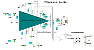
Notes :
Output Power : 200Watts
Load Resistance : 8ohms
Input impedance : 55K
Maximum supply voltage : (+95v)-0-(-95v)
Recommended supply voltage : (+66v)-0-(-66v)
Electronic Smart Heater Controller
This gadget can be used as an efficient and safe heater in living rooms, incubators, heavy electric/electronic instrument etc. Normally, when the temperature is below a set value (Decided by multi-turn preset pot P1), voltage at the inverting input (pin2) of IC1 is lower than the level at the non-inverting terminal (pin3). So, the comparator output (at pin 6) of IC1 goes high and T1 is triggered to supply mains power to the desired heater element.
Electronic Heater Controller Circuit diagram:

Note: CA3140 (IC2) is highly sensitive to electrostatic discharge (ESD). Please follow proper IC Handling Procedures.
When the temperature increases above the set value, say 50-60 degree centigrade, the inverting pin of IC1 also goes above the non-inverting pin and hence the comparator output falls. This stops triggering of T1 preventing the mains supply from reaching the heater element. Fortunately, the threshold value is user-controllable and can be set anywhere between 0 to 100 Degree centigrade.
The circuit works off stable 9Volt dc supply, which may be derived from the mains supply using a standard ac mains adaptor (100mA at 9V) or using a traditional capacitive voltage divider assembly. You can find such power circuits elsewhere in this website.
Digital Bike Tachometer
The tachometer circuit works according to this principle; the pulses created by the reed contacts are counted within a certain time interval. The resulting count is then displayed and represents the speed of the bike. Two 4026 ICs are used to count the pulses, decode the counter and control two 7-segment LED display. RS flip-flops U3 and U4 function as anti-bounce.
Electronic bicycle DIY tachometer Circuit diagram:

The pulses arrive at the counter’s input through gate U7. The measuring period is determined by monostable multivibrator U5/U6 and can be adjusted through potentiometer P1 so that the tacho can be calibrated. The circuit U1/U2 resets the counters.
Since batteries are used to power the circuit, it is not practical to support the continuous display of speed information. This circuit is not continuously active. The circuit is activated only after a button is pressed. At least three permanent magnets must be installed on the wheel. The circuit can be calibrated with the help of another pre-calibrated tachometer.
IR Remote Control Extender Mark 2
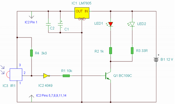
Notes:
The main difference between this version and the previous circuit, is that this design uses a commercially available Infra Red module. This module, part number IR1 is available from Harrison Electronics in the UK. The IR module contains a built in photo diode, amplifier circuit and buffer and decoder. It is centerd on the common 38kHz carrier frequency that most IR controls use. The module removes most of the carrier allowing decoded pulses to pass to the appliance. Domestic TVs and VCRs use extra filtering is used to completely remove the carrier. The IR1 is packaged in a small aluminium case, the connections viewed from underneath are shown below:
Infra Red Module, IR1 Pinout
How It works:
The IR1 module (IC3) operates on 5 Volt dc. This is provided by the 7805 voltage regulator, IC1. Under quiescent (no IR signal) conditions the voltage on the output pin is high, around 5 volts dc. This needs to be inverted and buffered to drive the IR photo emitter LED, LED2. The buffering is provided by one gate (pins 2 & 3) of a hex invertor the CMOS 4049, IC2. The IR1 module can directly drive TTL logic,but a pull-up resistor, R4 is required to interface to CMOS ICs. This resistor ensures that the signal from a remote control will alternate between 0 and 5 volts. As TTL logic levels are slightly different from CMOS, the 3.3k resistor R4 is wired to the +5 volt supply line ensuring that the logic high signal will be 5 volts and not the TTL levels 3.3 volts. The resistor does not affect performance of the IR module, but DOES ensure that the module will correctly drive the CMOS buffer without instability.
The output from the 4049 pin 2 directly drives transistor Q1, the 10k resistor R1 limiting base current. LED1 is a RED LED, it will flicker to indicate when a signal from a remote control is received. Note that in this circuit, the carrier is still present, but at a reduced level, as well as the decoded IR signal. The CMOS 4049 and BC109C transistor will amplify both carrier and signal driving LED2 at a peak current of about 120 mA when a signal is received. If you try to measure this with a digital meter, it will read much less, probably around 30mA as the meter will measure the average DC value, not the peak current. Any equipment designed to work between 36 and 40kHz should work, any controls with carrier frequencies outside this limit will have reduced range, but should work. The exception here is that some satellite receivers have IR controls that use a higher modulated carrier of around 115KHz. At present, these DO NOT work with my circuit, however I am working on a Mark 3 version to re-introduce the carrier.
Parts List:
C1 100u 10V
C2 100n polyester
R1 10k
R2 1k
R3 33R 1W
R4 3k3
Q1 BC109C
IC1 LM7805
IC2 CMOS 4049B
IC3 IR1 module from Harrison Electronics See Last paragraph
LED1 Red LED (or any visible colour)
LED2 TIL38 or part YH70M from Maplin Electronics
Testing:
This circuit should not present too many problems. If it does not work, arm yourself with a multimeter and perform these checks. Check the power supply for 12 Volt dc. Check the regulator output for 5 volt dc. Check the input of the IR module and also Pin 1 of the 4049 IC for 5 volts dc. With no remote control the output at pin 2 should be zero volts. Using a remote control pin 2 will read 5 volts and the Red LED will flicker. Measuring current in series with the 12 volt supply should read about 11mA quiescent, and about 40/50mA with an IR signal. If you still have problems measure the voltage between base and emitter of Q1. With no signal this should be zero volts, and rise to 0.6-0.7 volts dc with an IR signal. Any other problems, please email me, but please do the above tests first.
PCB Template:
Once again a PCB template has been kindly drafted for this project by Domenico.


The part number IR1 from Harrison Electronics is no longer available. They do supply an alternative IR decoder which I have tested and works. Other alternative Infrared decoders are shown below, note however that all DO NOT share the same pinout. I advise anyone making this to check the corresponding data sheets.
Vishay TSOP 1738
Vishay TSOP 1838
Radio Shack 276-0137
Sony SBX 1620-12
Sharp GP1U271R
Equipment Controlled Successfully:
If you have built this circuit and it works successfullt please let me know and I will build the list. Email details of the Manufacturer, device and remote control model number. The remote model number is usually on the front or back of the remote.
Technics CDP770 Remote: EUR64713
Tuesday, September 3, 2013
Linear Resistance Meter Circuit

Most linear scale resistance meters including the present design, work on the principle that if a resistance is fed from a constant current source the voltage developed across that resistance is proportional to its value. For example, if a 1K resistor is fed from a 1 mA current source from Ohm’s Law it can be calculated that 1 volt will be developed across the resistor (1000 Ohms divided by 0.001 amps = 1 volt). Using the same current and resistance values of 100 ohms and 10K gives voltages of 0.1volts (100 ohms / 0.001amps = 0.1volts) and 10 volts (10000 ohms / 0.001amps = 10 volts).
Thus the voltage developed across the resistor is indeed proportional to its value, and a voltmeter used to measure this voltage can in fact be calibrated in resistance, and will have the desired forward reading linear scale. One slight complication is that the voltmeter must not take a significant current or this will alter the current fed to the test resistor and impair linearity. It is therefore necessary to use a high impedance voltmeter circuit.
The full circuit diagram of the Linear Resistance Meter is given in Figure 1. The constant current generator is based on IC1a and Q1. R1, D1 and D2 form a simple form a simple voltage regulator circuit, which feeds a potential of just over 1.2 volts to the non-inverting input of IC1a. There is 100% negative feedback from the emitter of Q1 to the inverting input of IC1a so that Q1’s emitter is stabilised at the same potential as IC1a’s non-inverting input. In other words it is stabilised a little over 1.2 volts below the positive supply rail potential. S3a gives 5 switched emitter resistances for Q1, and therefore 5 switched emitter currents. S3b provides 5 reference resistors across T1 & T2 via S2 to set full-scale deflection on each range using VR1.
As the emitter and collector currents of a high gain transistor such as a BC179 device used in the Q1 are virtually identical, this also gives 5 switched collector currents. By having 5 output currents, and the current reduced by a factor of 10 each time S3a is moved one step in a clockwise direction, the 5 required measuring ranges are obtained. R2 to R6 must be close tolerance types to ensure good accuracy on all ranges. The high impedance voltmeter section uses IC1b with 100% negative feedback from the output to the inverting input so that there is unity voltage gain from the non-inverting input to the output. The output of IC1b drives a simple voltmeter circuit using VR1 and M1, and the former is adjusted to give the correct full-scale resistance values.
The CA3240E device used for IC1 is a dual op-amp having a MOS input stage and a class A output stage. These enable the device to operate with the inputs and outputs right down to the negative supply rail voltage. This is a very helpful feature in many circuits, including the present one as it enables a single supply rail to be used where a dual balanced supply would otherwise be needed. In many applications the negative supply is needed simply in order to permit the output of the op-amp to reach the 0volt rail. In applications of this type the CA3240E device normally enables the negative supply to be dispensed with.
As the CA3240E has a MOS input stage for each section the input impedance is very high (about 1.5 million Megohms!) and obviously no significant input current flows into the device. This, together with the high quality of the constant current source, and the practically non-existent distortion through IC1b due to the high feedback level gives this circuit excellent linearity.
With no resistor connected across T1 & T2 M1 will be taken beyond full-scale deflection and overloaded by about 100 or 200%. This is unlikely to damage the meter, but to be on the safe side a push-to-test on/off switch (S1) is used. Thus the power is only applied to the circuit when a test resistor is connected to the unit, and prolonged meter overloads are thus avoided.
A small (PP3 size) 9 volt battery is a suitable power source for this project which has a current consumption of around 5mA and does not require a stabilised supply.


e-mail: portagepal@tiscali.co.uk
Source: http://www.electronics-lab.com